
Chip Heat Flux W/cm² Puts the H100 at Air Cooling’s Edge
Electronics Cooling’s 2005 comparison of air and liquid options for a four-chip module concluded that indirect liquid cooling removes two to four times the chip heat flux that air does. For a current accelerator the claim holds in part. NVIDIA’s published power and die area put the H100 SXM at an average of 86.0 W/cm², just above the 60 to 84 W/cm² that study calculated for its air-cooled module. This piece covers average die heat flux for parts with published power and die area, and leaves out hot spots and rack airflow, because none of the documents opened here maps hot spots and the rack side is a separate question taken up in the air cooling limit per rack.
Dividing rated power by die area puts the H100 SXM at 86.0 W/cm²
Heat flux in this piece means rated power divided by die area, q = P ÷ A. The power is the thermal design power (TDP) a vendor publishes for the part, and the area is the die size it publishes for the GPU. The quotient is an average over the die. It says nothing about the hottest square millimeter, and it treats all of the rated power as entering through the die footprint.
NVIDIA’s H100 product page lists a maximum TDP of up to 700W (configurable) for the SXM form factor. The company’s Hopper architecture post gives the die size as 814 mm² but marks its H100 specifications as preliminary, so the power figure here comes from the product page.
Conversion: 814 mm² ÷ 100 = 8.14 cm². Result: q = 700 W ÷ 8.14 cm² = 86.0 W/cm². Because the operator can set the power limit below 700 W, this is an upper bound for the module and not a typical operating value.
The same Hopper post tabulates the A100 at 400 W and 826 mm², which gives 48.4 W/cm².
Between the two parts power rose by a factor of 1.75 and die area fell by 1.5%, so the flux rose by a factor of 1.78. Nearly all of the increase came from watts.
Table 1. Average heat flux from published rated power and die area (W/cm²)
| Part | Rated power (W) | Die area (mm²) | Heat flux (W/cm²) |
|---|---|---|---|
| NVIDIA H100 SXM | up to 700 | 814 | 86.0 |
| NVIDIA H100 NVL (PCIe, dual slot, air-cooled) | 350 to 400 | 814* | 43.0 to 49.1 |
| NVIDIA A100 | 400 | 826 | 48.4 |
| Graphcore MK2 IPU | 300 | 832 | 36.1 |
* NVL die area is an assumption, taken from the GH100 value in the Hopper post (no NVL die size found); power is a configurable maximum; flux = power ÷ die area, an average with no hot spot
Source: NVIDIA, “NVIDIA Hopper Architecture In-Depth” (2022) and H100 product page; Jouppi et al., “TPU v4” (ISCA 2023); flux calculated for this piece
The H100 NVL, which the product page lists as a PCIe dual-slot air-cooled card at 350-400W (configurable), works out to 43.0 to 49.1 W/cm² if its die area is assumed to be the same 814 mm²; the product page gives no die size for the NVL card, so that area is an assumption. That is the A100’s flux class and below the bottom of the 2005 air range.
Google’s TPU v4 paper, in a table comparing competing accelerators, gives the Graphcore MK2 IPU as 832 mm² and 300 W, or 36.1 W/cm².
With die area holding near 800 mm² across these parts, a designer who tracks watts per socket is tracking flux.
The 2005 air range comes from a 60 K budget across a four-chip module
No figure of 100 W/cm² appears in the Electronics Cooling article. Its air results run from 60 to 84 W/cm², and it adds that the number would fall if some of the blower flow had to cool other parts in the drawer.
The article also quotes an earlier desktop result by Saini and Webb, a 16 × 16 mm source with a 35°C difference to inlet air, that allowed 37.2 W/cm², so the configuration decides much of the range.
The module analysis used four 12.25 × 12.25 mm chips on a 42.5 × 42.5 mm substrate, with module plus cooler held under 89 mm so that it fits a drawer two EIA units high.
Maximum chip temperature was 85°C and coolant or air inlet was 25°C, a 60 K difference.
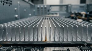
The air path was an 80 × 80 × 4 mm vapor chamber base under parallel plate fins, aluminum or copper, 0.381 mm thick and 60 mm tall.
Two radial blowers in parallel supplied 0.0217 m³/s (45.9 CFM) at 141.4 Pa through the fins.
At module level the heat sink resistance came out at 0.10°C/W with aluminum fins and 0.069°C/W with copper.
Chip-to-base resistance, including the silicon and a thermal interface, was 0.267°C/W with thermal paste and 0.20°C/W with solder.
The page text does not show the article’s Equation (1). A series-resistance form, P = ΔT ÷ (R_c-hs + 4 × R_hs) per chip, with the 4 because four chips share one sink, reproduces both published endpoints. Chip area is 12.25 mm × 12.25 mm = 150.06 mm², or 1.5006 cm².
Aluminum fins with paste: P = 60 K ÷ (0.267 + 4 × 0.10) °C/W = 89.96 W, so q = 89.96 W ÷ 1.5006 cm² = 59.9 W/cm².
Copper fins with solder: P = 60 K ÷ (0.20 + 4 × 0.069) °C/W = 126.05 W, so q = 126.05 W ÷ 1.5006 cm² = 84.0 W/cm².
Both results are modeled maximum uniform fluxes for that module, which makes 84.0 W/cm² an upper bound for air in that envelope.
Multiplying resistance by area turns the best case into a unit resistance that can be compared across die sizes, a quantity treated in how to read a thermal resistance rating. For the copper and solder case, R″ = 0.476 °C/W × 150.06 mm² = 71.4 °C·mm²/W.
The H100 SXM under the same 60 K budget at 700 W allows R = 60 K ÷ 700 W = 0.0857 °C/W, and R″ = 0.0857 °C/W × 814 mm² = 69.8 °C·mm²/W.
The module would need a unit resistance 2.3% below the study’s best air case. On the study’s own terms the H100 SXM sits just past the edge of air, not several multiples beyond it. The 60 K budget is the article’s assumption and not an NVIDIA specification, and the sources opened here give no case temperature limit for the H100.
Does an air-cooled 700 W system break the 84 W/cm² ceiling?
It does not, because the ceiling belongs to the study’s envelope and not to physics. NVIDIA’s DGX H100/H200 guide describes an 8U rackmount, 14 in (356 mm) tall.
Its environmental table lists airflow of 1105 CFM front to back at 80% fan PWM and an operating temperature of 5°C to 30°C.
AMD’s Hot Chips 2024 MI300X deck describes the DGX H100 in its benchmark footnotes as 8x NVIDIA H100 (80GB, 700W) GPUs.
Air cooling does serve 700 W parts, then, in a chassis four times the height of the 89 mm module.
The inlet range reaches 30°C against the study’s 25°C, and the guide gives no GPU temperature limit to compare.
ASHRAE TC9.9’s 2021 white paper on liquid cooling in mainstream data centers frames the same trade from the other side. It says that as socket power moves through 300 W toward 400 W, standard 1U and 2U servers become more difficult to cool with air.
The 2005 module was a drawer two EIA units high, so both documents point at the same low-profile form factors, and the 8U chassis shows what air costs once past them: volume.
The white paper names a second pressure. Case temperature requirements are falling, and it expects them to reach the low 70°C range for some parts, especially CPUs with high-bandwidth memory.
Illustration with an assumed 70°C case limit and 25°C inlet, which leaves 45 K, holding the study’s best air resistance fixed: q = 45 K ÷ 71.4 °C·mm²/W = 0.630 W/mm² = 63.0 W/cm².
The air ceiling moves down by a quarter in that illustration while die flux moves up.
Cold plates in the same study carry 2.7 to 4.7 times the best air figure
Under the same 60 K difference, Electronics Cooling calculated chip heat removal of 227 W/cm² for a separable module cold plate, 320 W/cm² for an integral module cold plate and 397 W/cm² for chip-scale cold plates.
Its prose summarizes this as two to four times air. Against the 60 W/cm² air result the cold plate figures are 3.8 to 6.6 times higher, and against 84 W/cm² they are 2.7 to 4.7 times, so the prose is looser than the article’s own numbers.
Table 2. Modeled chip heat flux at a 60 K chip-to-fluid difference, with the H100 SXM for scale (W/cm²)
| Cooling option (Electronics Cooling, 2005) | Type | Heat flux (W/cm²) |
|---|---|---|
| Water jet impingement | Direct, water* | 460 |
| Chip-scale cold plate | Indirect liquid | 397 |
| Integral module cold plate | Indirect liquid | 320 |
| Dielectric microchannel heat sink on chip | Direct, dielectric | 300 |
| Separable module cold plate | Indirect liquid | 227 |
| Dielectric jet impingement | Direct, dielectric | 120 |
| NVIDIA H100 SXM, 700 W ÷ 814 mm² (this piece)** | Average, rated power | 86.0 |
| Parallel plate fin heat sink, four-chip module | Air | 60 to 84 |
| Dielectric spray cooling | Direct, dielectric | 60 |
* Assumes a seal that keeps water off the interconnects; calculated values, not measurements
** Not part of the study; an average from rated power, not a modeled maximum uniform flux
Source: Electronics Cooling, “High Powered Chip Cooling — Air and Beyond” (2005); NVIDIA H100 product page and Hopper architecture post
The mechanism is channel size. ASHRAE TC9.9’s 2019 water-cooled servers white paper says the microchannel cold plate is the most commonly used liquid heat transfer device in electronics cooling, with fin spacing often less than a few tenths of a millimeter. The same paper notes that narrower spacing improves heat transfer at the cost of static pressure drop across the plate.
A review by Agostini and colleagues, published in Heat Transfer Engineering in 2007, gives 300 W/cm² below 85°C as the objective for the next chip generation. It reports that EPFL’s laboratory reached 200 W/cm² in a first prototype. The first is a research objective and the second a laboratory prototype result, and the Electronics Cooling values are calculations rather than measurements on shipping hardware.
On those terms the H100 SXM’s 86.0 W/cm² is 38% of the separable cold plate figure of 227 W/cm²
It is 22% of the chip-scale figure of 397 W/cm².
The remaining 2.6 to 4.6 times of margin is a rough screen for non-uniform power and not a hot spot calculation, and it is the margin air no longer has at this die.
Doubts that remain about a flux calculated from rated power
Is 86.0 W/cm² the flux at the hottest spot?
No. It is rated power spread evenly over 8.14 cm², which is also how the 2005 study posed its limits, as maximum uniform heat flux. Neither the Hopper post nor the product page publishes a power map, so a local peak cannot be computed from them. Somewhere on a real die the local flux exceeds the average, and by how much is a matter for the vendor’s thermal design documents.
Why does Table 1 stop at the H100, the A100 and one IPU?
The sources opened here give both power and die area for those parts only. AMD’s Hot Chips 2024 deck lists 750W for the MI300X in its footnotes but shows no die areas in the text read, and a package of several dies has no single area to divide by.
Can 60 to 84 W/cm² serve as a design limit for air?
No. It is a modeled maximum for one drawer-sized module with specific fins, blowers and a 60 K budget, and the article itself says the figures should be read in relative terms. Thermal design for a real chassis, inlet temperature and chip needs qualified engineering review against the vendor’s own limits.
The data place the H100 SXM at the edge of the air range
The H100 SXM works out to 86.0 W/cm² on rated power, just above the 60 to 84 W/cm² that a 2005 module study calculated for air. Air-cooled 700 W systems exist because a taller chassis and a different budget move the envelope, so these documents do not support the claim that liquid is required at this flux, while they do support the claim that liquid has far more headroom, with modeled cold plate figures of 227 to 397 W/cm². Die area has held roughly constant across these parts, so each TDP step carries the flux with it, and a falling case temperature limit shrinks the air side at the same time.
References
- High Powered Chip Cooling — Air and Beyond / Electronics Cooling / 2005 / https://www.electronics-cooling.com/2005/08/high-powered-chip-cooling-air-and-beyond/
- NVIDIA Hopper Architecture In-Depth / NVIDIA Technical Blog / 2022-03-22 / https://developer.nvidia.com/blog/nvidia-hopper-architecture-in-depth/
- NVIDIA H100 GPU product page / NVIDIA / undated / https://www.nvidia.com/en-us/data-center/h100/
- Introduction to NVIDIA DGX H100/H200 Systems / NVIDIA DGX documentation / undated / https://docs.nvidia.com/dgx/dgxh100-user-guide/introduction-to-dgxh100.html
- AMD Instinct MI300X Generative AI Accelerator and Platform Architecture / AMD, Hot Chips 2024 / August 2024 / https://hc2024.hotchips.org/assets/program/conference/day1/23_HC2024.AMD.MI300X.ASmith(MI300X).v1.Final.20240817.pdf
- TPU v4: An Optically Reconfigurable Supercomputer for Machine Learning with Hardware Support for Embeddings / Google, ISCA 2023 / 2023 / https://arxiv.org/pdf/2304.01433
- Emergence and Expansion of Liquid Cooling in Mainstream Data Centers / ASHRAE TC9.9 / 2021 / https://www.ashrae.org/file%20library/technical%20resources/bookstore/emergence-and-expansion-of-liquid-cooling-in-mainstream-data-centers_wp.pdf
- Water-Cooled Servers: Common Designs, Components, and Processes / ASHRAE TC9.9 / 2019 / https://www.ashrae.org/file%20library/technical%20resources/bookstore/whitepaper_tc099-watercooledservers.pdf
- State of the Art of High Heat Flux Cooling Technologies, Heat Transfer Engineering (abstract only) / IBM Research publication record / 2007 / https://research.ibm.com/publications/state-of-the-art-of-high-heat-flux-cooling-technologies





댓글 0
첫 댓글을 남겨보세요.